
Reduce the risk of missing key data
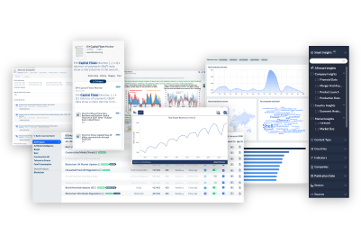
by automating your MI and CI tasks. With ReportLinker, you can simultaneously track multiple companies, sectors, topics and territories across countless sources.
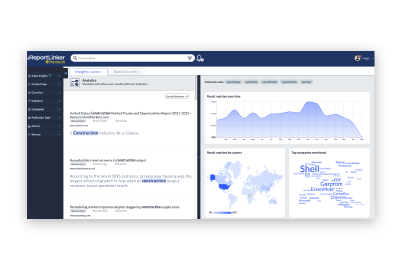
Gain insight into complex environments quickly through analysis and representation
Producing accurate intelligence outputs is crucial to enable well-informed decision-making.
With Reportlinker, it is now possible in a matter of seconds, thanks to the combination of our powerful proprietary AI and GPT.
Our AI is specifically designed to detect insights and complete intelligence tasks, allowing us to quickly and accurately produce intelligence deliverables tailored to the needs of any stakeholders, from marketing and sales teams to executives and corporate strategy teams.
Learn moreby automating your MI and CI tasks. With ReportLinker, you can simultaneously track multiple companies, sectors, topics and territories across countless sources.
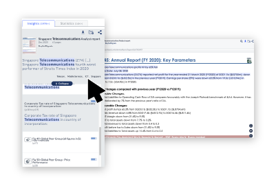
with AI trained to understand business and competitive contexts. ReportLinker allows you to go beyond keyword searches and deliver insights with unprecedented accuracy.
with learning algorithms trained to detect early signals. ReportLinker helps you stay ahead of competitors and drive innovation through out your organization.
Complete tool for marketing intelligence. Research can be very focused and detailed, and also the translation intelligence of the tool makes a difference.
ReportLinker’s platform allows us to do in-depth research on the context and state of an industry, on the market trends in a specific country, as well as on a global level. Read the full case study
Great tool for Market Intelligence… Having the capability to add our own websites adds a lot of personalization to our searches and makes our market intelligence research easier.
My team needed to find information faster and ReportLinker allows them to focus on the right information and not waste time on irrelevant sources. Read the full case study
A straightforward and intuitive platform that facilitates one's market research process needs.
ReportLinker is a huge help in market watch and prospection related issues specifically regarding innovative sectors relevant to us.
Excellent source of Industry information
The Smart Insights function is one of the better features / enhancements of ReportLinker. It allows one to filter and obtain the most relevant results easily and fast.
With the Smart Insight trackers, I can easily find the competitors in a market. I can also sort the data by country, by company and have a complete understanding of any industry’s current trends. Read the full case study
The key benefit is speed. We divided by two our online research time since we started using ReportLinker. Read the full case study
Ready to eliminate Information overload and the risk of missing key data?


Comprehensive collection of guides, webinars & articles to help you learn more about AI-powered Intelligence and automation

Our challenge? Reinventing Intelligence with Technology